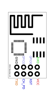
In this post I describe the way I have designed and built a simple and useful development board for ESP8266–01
Image may be NSFW.
Clik here to view.
Clik here to view.

The main goal of this board is to make the use of ESP8266–01 simple during development phase on breadboard.
Schema
The schema is quite simple.
A detailed explanation on how to correctly connect EPS8266–01 pins is available here [http://www.instructables.com/id/How-to-use-the-ESP8266-01-pins/?ALLSTEPS]
Image may be NSFW.
Clik here to view.
Clik here to view.
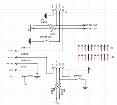
The pinheader J1 and J2, in the above electrical schema, are the 8 pin of the ESP8266–01 module (as seen from above view)
Image may be NSFW.
Clik here to view.
Clik here to view.
The 5 pin on the left, in the above electrical schema, are the pin of the dev board. More in detail:
- VCC: 3V3 (+) from a couple of AA batteries or any other power source (in the schema is writte 5V as I was not able to change it in Fritzing)
- GND: the negative (-) wire from the two AA batteries or from any DC 3V3 power source
- USB GND: the ground from the USB2TTL module
- USB RX/TX: RX/TX from the USB2TTL module
The two pin top-right are the GPIO0 and PIO2 available on the ESP8266–10 module
The pin header J3 and J4 are not electrically connected and wired and are only used to mount the dev board on the breadboard
Two micro-buttons are available to reset the ESP8266–01 module (SW RST) and to switch into flashing/programming mode (SW GPIO0)
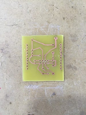
PCB
The PCB has been made using Fritzing software and is a single side PCB for an easy development at home
Image may be NSFW.
Clik here to view.
Clik here to view.
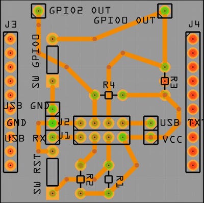
Image may be NSFW.
Clik here to view.
Clik here to view.
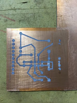
Making the PCB
I have use a home made development process to build the PCB which is called “toner transfer”. In short I have printed the circuit on glossy photo paper with a laser printer and later transferred the PCB tracks on the copper clad with a normal iron (borrowed from my wife :) )
Image may be NSFW.
Clik here to view.
Clik here to view.
The result is not 100% perfect (doing that at home with basic tools) as half track and few pad have not been transferred correctly
Image may be NSFW.
Clik here to view.
Clik here to view.
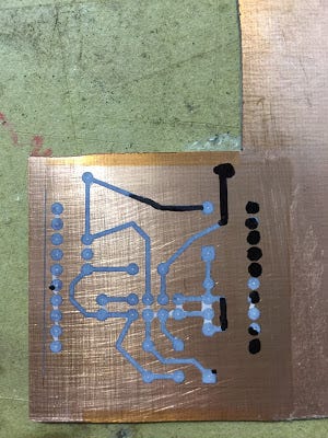
No worries, we are maker so we always find a solution. I have manually corrected the missing toner with a permanent maker (the pad which are missing are the one which are not electrically connected so no big issue)
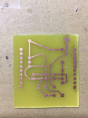
Below the final result after the copper etching
Image may be NSFW.
Clik here to view.
Clik here to view.
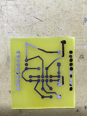
Now I remove the toner with some simple acetone (borrowed from my wife)
Image may be NSFW.
Clik here to view.
Clik here to view.
now I drill the board with a 1mm drill bit
Image may be NSFW.
Clik here to view.
Clik here to view.
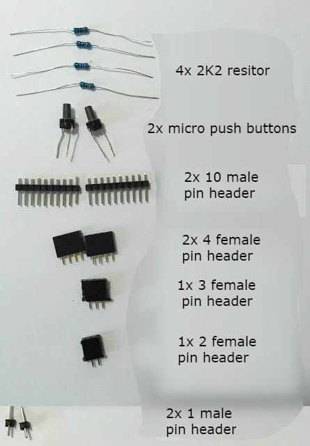
Assembling the Board
Now it is time to assemble the board with just few components
Here the list of components:
Image may be NSFW.
Clik here to view.
Clik here to view.
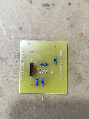
I start by soldering the resistors, the pin header and then the push buttons
Image may be NSFW.
Clik here to view.
Clik here to view.
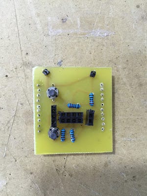
Below the final result
Image may be NSFW.
Clik here to view.
Clik here to view.
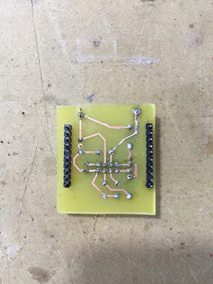
Image may be NSFW.
Clik here to view.
Clik here to view.
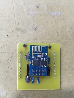
and also with ESP8266–01 module
Image may be NSFW.
Clik here to view.
Clik here to view.
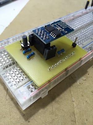
and everything mounted on breadboard
Image may be NSFW.
Clik here to view.
Clik here to view.

Image may be NSFW.
Clik here to view.
Clik here to view.
File
The full fritzing project with electrical schema and PCB layout is available here qui
Suggestion
The two pin header rows on the side of the dev board, are slightly larger than the breadboard. In order to overcame this small issue I have removed the 6th pin from the row.
In version 2 of this board I will fix this bug but until then I can use the dev board with the small trick explained above.
This allows me to work on my project base don ESP8266–01 in a clean and easy way avoiding flying wires.
Image may be NSFW.
Clik here to view.